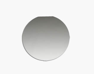
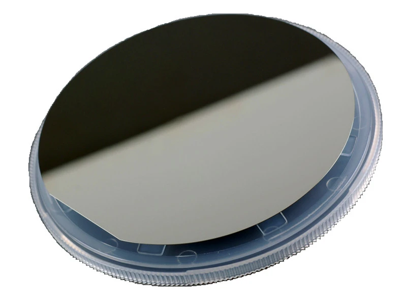
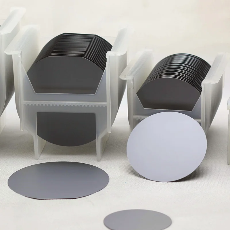
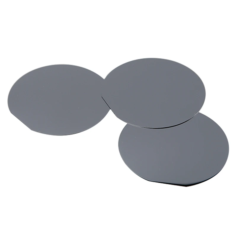
4 Inch Silicon Wafer
As supplements platforms such as LiNbO 3 Si 3 N 4 etc. The company is also developing new semiconductor wafer materials also known as third-generation and fourth-generation.
T Siw 4 Nanoandmore
The as-received Al 2 O 3 0001 substrate 10 10 mm or 2-inch c-plane and double-side polished from 11-D Tech was cleaned sequentially with acetone isopropanol and deionized water for 5 min.

. The process began with the growth of a bilayer MoS 2 thin film thickness 14 nm on the 4 inch GaN epitaxial wafer coated with an insulating SiO 2 buffer layer via metalorganic chemical. The dicing process can involve scribing and breaking mechanical sawing normally with a machine called a dicing saw or laser cuttingAll methods are typically automated to ensure precision and. The OV9281 has a chief ray angle CRA of 9 degrees and comes in a chip scale package.
Starting from the top in terms of their Arm-architecture CPU cores the M2 retains Apples 4 performance plus 4 efficiency core configuration. The OV9281 and OV9282 also feature support for frame synchronization and dynamic defective pixel correction. The research team built the cell on a 4-inch wafer scale by applying a microgrid electrode with a uniform square pattern array with a width of 34 µm and a spacing of 400 µm.
GlobalWafers yesterday confirmed that it would break ground for a planned 12-inch silicon wafer fab in Texas at the end of November following the passage of the Creating Helpful Initiatives to Produce Semiconductors and Science Act in the US. In the context of manufacturing integrated circuits wafer dicing is the process by which die are separated from a wafer of semiconductor following the processing of the wafer. The 14-inch OV9281 and OV9282 capture 1280 x 800 resolution images at 120 frames per second fps and VGA resolution at 180 fps with 2-lane MIPI and DVP output.
In electronics a wafer also called a slice or substrate is a thin slice of semiconductor such as a crystalline silicon c-Si used for the fabrication of integrated circuits and in photovoltaics to manufacture solar cellsThe wafer serves as the substrate for microelectronic devices built in and upon the wafer. It undergoes many microfabrication processes such as doping ion. Apple is not disclosing what generation CPU cores.
However traditional silicon photonics cannot realize all functions required by information society.
4 Inch Sio2 Silicon Dioxide Wafer Resistivity 10000 Ohms Cm Model Double Oxygen Silicon Wafer Thickness 500um Flanges Aliexpress
4 Inch Sio2 Silicon Dioxide Wafer Resistivity 8 12 Ohms Cm Silicon Wafer Thickness 525um Double Oxygen Flanges Aliexpress
Silicon Wafer 4 100mm P Boron Prime 25 Pack Pi Kem
4 Inch Silicon Wafer Ic Semiconductor Grade High Purity Single Crystal Polished Silicon Wafer Electron Microscope Sem Instrument Parts Accessories Aliexpress
0 Response to "4 Inch Silicon Wafer"
Post a Comment